
Major Advancement in Applied Research: FMD Launches the Chiplet Application Hub
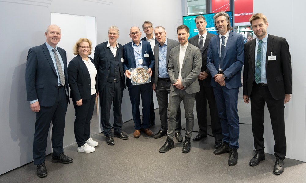
On March 31, 2025, at the Hannover Messe, the Research Fab Microelectronics Germany (Forschungsfabrik Mikroelektronik Deutschland FMD) officially unveiled its new Chiplet Application Hub. Designed to serve as a central platform for the development and application of chiplet technologies, the hub aims to bridge the gap between research and industrial use. By working closely with industry partners, the hub accelerates the development of chiplets made in Germany, elevating industrial research to a new level. At the national level, it complements FMD’s role in the Chips for Europe Initiative, further reinforcing Germany’s technological resilience. The hub's research, development, and prototyping activities build on the infrastructure of the APECS pilot line, ensuring direct pathways to industrial application.
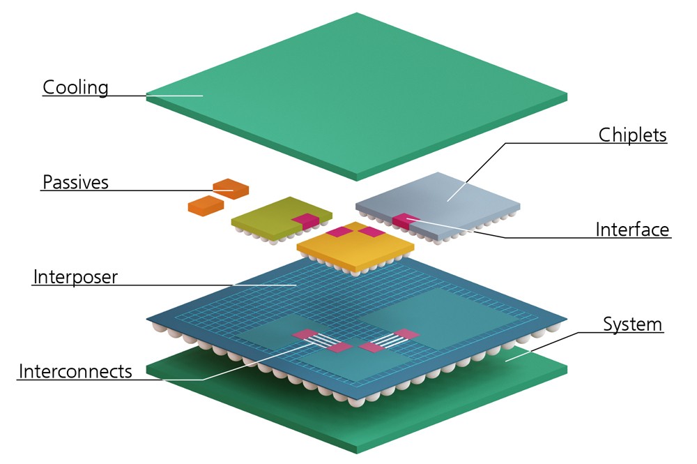
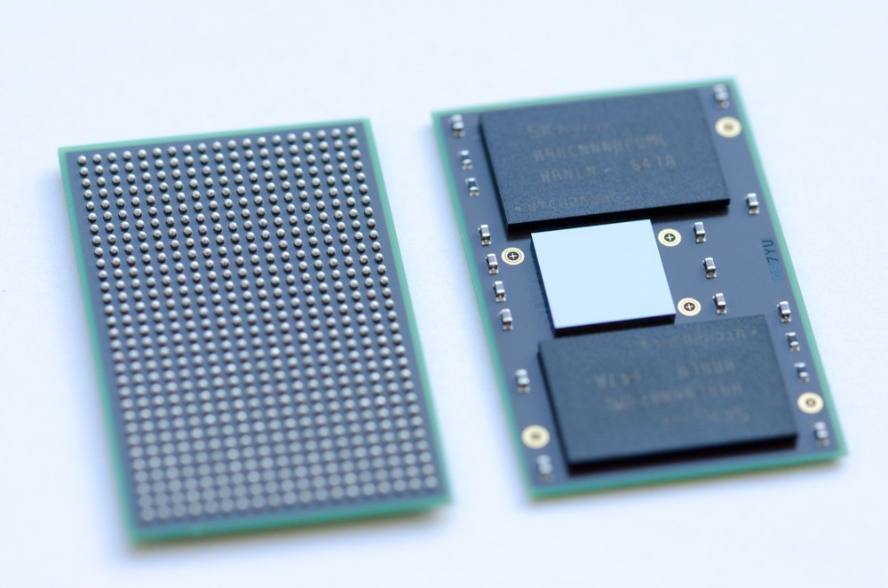
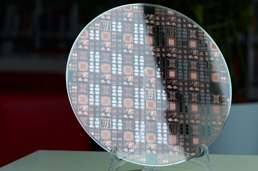
The Research Fab Microelectronics Germany (FMD) works intensively in the field of heterogeneous integration and is helping to drive chiplet innovation at the European level through the APECS pilot line, which was launched at the end of 2024. Of the total of €730 million in funding allocated for APECS, a significant percentage will be dedicated to the technological development of chiplets. These technologies open up groundbreaking opportunities, particularly for the automotive industry and high-performance computing, as well as for other sectors such as industrial electronics and medical devices. Chiplets support advances in areas such as advanced packaging and the integration of high-performance subsystems, including powerful computing modules, sensor or edge modules, and control units. They also contribute to a more flexible supply chain by enabling the use of semiconductor components from different manufacturers.
To strategically strengthen the industrial use of chiplets in Germany and across Europe, the FMD is establishing the Chiplet Application Hub. The hub will serve as the operational framework for the APECS pilot line, ensuring that companies gain access to the latest chiplet advancements while supporting the continued consolidation of European semiconductor expertise. The FMD, together with industry partners from across the semiconductor ecosystem, is combining its expertise to jointly develop new chiplet solutions for applications in automotive and automation. These collaborative efforts will feed into targeted development roadmaps and pilot projects aligned with the specific needs of industry. In return, industry partners will play a key role in advancing chiplet innovation in close cooperation with the FMD. Combined with the technological capabilities of the APECS pilot line, this lays the foundation for new manufacturing technologies, design methods, and standards, as well as the testing of functional prototypes. As a catalyst for pre-competitive industrial research, the Chiplet Application Hub elevates these activities to a new level, accelerating the transfer of innovation into practical industrial use.
Chiplet technology as a catalyst for value creation, technology transfer and competitiveness
The importance of the chiplet technology lies in its modular and scalable nature. It enables the deliberate combination of different semiconductor technologies, allowing them to be tailored to specific applications. As a result, entirely new system architectures become feasible, bringing improvements in energy efficiency, performance, and the reusability of individual high-cost design components.
Prof. Holger Hanselka, President of the Fraunhofer-Gesellschaft, states: “The establishment of the Chiplet Application Hub marks a further milestone for microelectronics research in Germany. Europe will also benefit greatly from the development of an independent, high-performance semiconductor industry. Close cooperation between research and industry allows us to fully harness the innovative potential of chiplet technology.” Hanselka emphasizes that this effort exemplifies how strong partnerships between leading European research institutions and companies are essential to technological resilience and the foundation for groundbreaking innovations. He also notes that “the arrival of imec in Baden-Württemberg vividly demonstrates how strategic cross-border partnerships can sustainably enhance Europe's competitiveness.”
Prof. Albert Heuberger, chairman of the FMD steering committee, spokesperson for the Fraunhofer Group for Microelectronics, and founding director of the Chiplet Application Hub, elaborates: “The Chiplet Application Hub is a vital asset for implementing the EU Chips Act in Germany and will be closely linked to the competence centers being established across Europe under this initiative. imec’s decision to locate in Heilbronn highlights the strong integration of key players in the European chip ecosystem and illustrates how the EU Chips Act fosters collaboration across RTOs, companies, and competence centers to advance Europe’s position in semiconductor innovation.”
Voices from the industry: The advantages of a strategic partnership with the Chiplet Application Hub
At the core of the Chiplet Application Hub is close collaboration with strong industry partners to develop practical, application-driven solutions. By combining design, system integration, and testing processes, the hub is intended to serve as a long-term platform for advancing chiplet technologies in Germany and across Europe. Modular semiconductor architectures hold significant potential, particularly in areas such as high-performance computing and artificial intelligence.
“Chiplet technology is a crucial building block for the future of the semiconductor industry,” says Dr. Heike Riel, an IBM Fellow who oversees the science of quantum and information technology at IBM. “Through the modular integration of semiconductor components, we can create innovative computing solutions that are not only more powerful, but also more energy efficient. The Chiplet Application Hub provides an ideal platform to further develop this technology and drive its industrial implementation.”
Similarly, in the automotive sector, chiplet technology is unlocking new opportunities for powerful and adaptable electronic systems.
Jürgen Heckelmann, Head of Strategic Semiconductor Management Procurement at Audi AG, welcomes the launch of the hub and says: “Chiplets offer major advantages for the automotive industry. As we move toward centralized control units, we need flexible and scalable solutions. For automated driving and infotainment in particular, chiplets allow precise customization across vehicle categories and functionalities. They also support more energy-efficient designs with lower power dissipation. Another key benefit is the modularization of sensor and actuator systems, which enhances flexibility in system integration. The hub will be a key partner in shaping future electronic architectures.”
Andreas Aal, Senior Member IEEE, CRP at Volkswagen Commercial Vehicles and Chair of the SEMI GAAC, explains: “Over the long term, chiplets give us the ability to tailor hardware platforms specifically for software-driven business models like Mobility and Transport-as-a-Service while ensuring flexibility, adaptability, and cost efficiency. The Chiplet Application Hub is a key enabler, helping us transfer digital innovations from outside the automotive sector into vehicles, particularly in areas such as life cycle management, cybersecurity, and system robustness. To achieve this, we must move beyond the traditional automotive ecosystem and evolve into a resilient system of systems aligned with the global digital landscape.”
By combining industrial research with technology transfer, the Chiplet Application Hub is set to drive innovation and accelerate the market adoption of chiplet technologies. In the years ahead, targeted collaborations, research initiatives, and the development of a strong innovation network will support the hub’s continued growth and contribute to strengthening Germany’s global competitiveness.
Strong partnerships for a strong chip ecosystem
With the launch of the Chiplet Application Hub, the FMD is underscoring the central role of chiplet technology in microelectronics research and strengthening its position within the European chip ecosystem. The planned arrival of leading research institutions, such as Belgium’s imec, further reflects the growing importance of this technology. imec plans to set up a research group in Heilbronn, Baden-Württemberg, to work on chiplet architectures for high-performance computing in the automotive sector. To move forward together, imec and the FMD have signed a memorandum of understanding (MoU) that outlines a shared strategic direction to fully tap the potential of chiplet technologies. The agreement reinforces their commitment to driving innovation and setting new standards for the development and industrial use of chiplets.
Download:
Last modified: